- 您现在的位置:买卖IC网 > Sheet目录17368 > NCP3011GEVB (ON Semiconductor)BOARD EVAL NCP3011 BUCK CTLR
�� �
�
�NCP3011,� NCV3011�
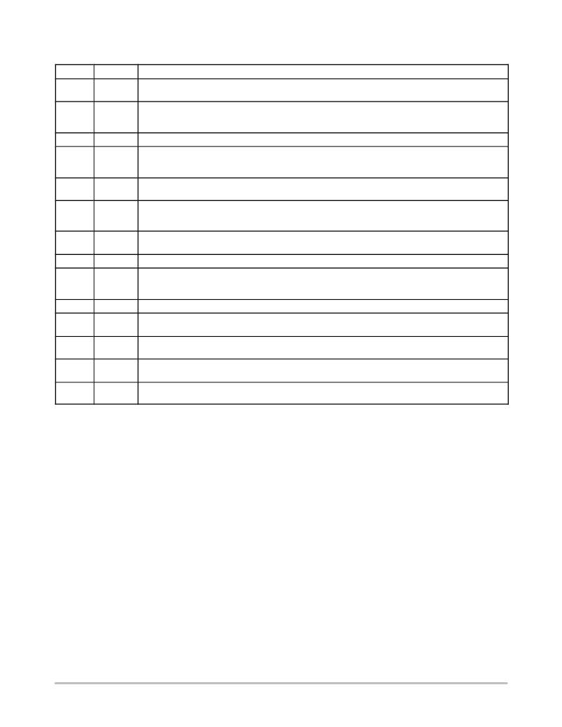
�PIN� FUNCTION� DESCRIPTION�
�Pin�
�1�
�2�
�3�
�4�
�5�
�6�
�7�
�8�
�9�
�10�
�11�
�12�
�13�
�14�
�Pin� Name�
�VREF�
�EN�
�NC�
�SYNC�
�PG�
�COMP�
�FB�
�GND�
�LSDR�
�NC�
�VSW�
�HSDR�
�BST�
�V� CC�
�Description�
�The� VREF� pin� is� the� output� for� a� 1.25� V� reference� (1� mA� max).� A� 100� k� W� resistor� in� parallel� with� a� 1� m� F�
�ceramic� capacitor� must� be� connected� from� this� pin� to� GND� to� ensure� external� reference� stability.�
�The� EN� pin� is� the� enable/disable� input.� A� logic� high� on� this� pin� enables� the� device.� This� pin� has� also� an� internal�
�current� source� pull� up.� A� 10� k� W� resistor� should� be� connected� in� series� with� this� pin� if� V� EN� is� externally� biased�
�from� a� separate� supply.�
�Not� Connected�
�The� dual� function� SYNC� pin� synchronizes� the� device� to� a� higher� frequency� (Slave� Mode).� Alternately,� it� outputs�
�a� 456� kHz� clock� signal� with� 180� °� of� phase� shift� (Master� Mode).� Connect� a� 100� k� W� resistor� from� SYNC� to� GND�
�to� enable� Master� Mode.� No� resistor� is� required� for� Slave� Mode.�
�The� Power� Good� pin� is� an� open� drain� output� that� is� low� when� the� regulated� output� voltage� is� beyond� the�
�“Power� Good”� upper� and� lower� thresholds.� Otherwise,� it� is� a� high� impedance� pin.�
�The� COMP� pin� connects� to� the� output� of� the� Operational� Transconductance� Amplifier� (OTA)� and� the� positive�
�terminal� of� the� PWM� comparator.� This� pin� is� used� in� conjunction� with� the� FB� pin� to� compensate� the� voltage�
�mode� control� feedback� loop.�
�The� FB� pin� is� connected� to� the� inverting� input� of� the� OTA.� This� pin� is� used� in� conjunction� with� the� COMP� pin� to�
�compensate� the� voltage� mode� control� feedback� loop.�
�Ground� Pin�
�The� LSDR� pin� is� connected� to� the� output� of� the� low� side� driver� which� connects� to� the� gate� of� the� low� side�
�N� ?� FET.� It� is� also� used� to� set� the� threshold� of� the� current� limit� circuit� (I� SET� )� by� connecting� a� resistor� from� LSDR�
�to� GND.�
�Not� Connected�
�The� VSW� pin� is� the� return� path� for� the� high� side� driver.� It� is� also� used� in� conjunction� with� the� V� CC� pin� to� sense�
�current� in� the� high� side� MOSFET.�
�The� HSDR� pin� is� connected� to� the� output� of� the� high� side� driver� which� connects� to� the� gate� of� the� high� side�
�N� ?� FET.�
�The� BST� pin� is� the� supply� rail� for� the� gate� drivers.� A� capacitor� must� be� connected� between� this� pin� and� the�
�VSW� pin.�
�The� V� CC� pin� is� the� main� voltage� supply� input.� It� is� also� used� in� conjunction� with� the� VSW� pin� to� sense� current�
�in� the� high� side� MOSFET.�
�http://onsemi.com�
�3�
�发布紧急采购,3分钟左右您将得到回复。
相关PDF资料
MIC2505BM
IC SW HIGH SIDE SGL 2A 8SOIC
MIC2505-2BM
IC SW HIGH SIDE SGL 2A 8SOIC
MIC2505-1BM
IC SW HIGH SIDE SGL 2A 8SOIC
TAAB106K020G
CAP TANT 10UF 20V 10% AXIAL
MC34063LBBEVB
EVAL BOARD FOR MC34063LBB
A9BAG-0502F
FLEX CABLE - AFF05G/AF05/AFE05T
EBM08DTMD-S189
CONN EDGECARD 16POS R/A .156 SLD
RCM06DSUI
CONN EDGECARD 12POS DIP .156 SLD
相关代理商/技术参数
NCP3012
制造商:ONSEMI 制造商全称:ON Semiconductor 功能描述:Synchronous PWM Controller
NCP3012DTBR2G
功能描述:电压模式 PWM 控制器 Single Output Buck 0.8V to 40V 70uA RoHS:否 制造商:Texas Instruments 输出端数量:1 拓扑结构:Buck 输出电压:34 V 输出电流: 开关频率: 工作电源电压:4.5 V to 5.5 V 电源电流:600 uA 最大工作温度:+ 125 C 最小工作温度:- 40 C 封装 / 箱体:WSON-8 封装:Reel
NCP301HSN09T1
功能描述:电压监测器/监控器 0.9V Detector RoHS:否 制造商:Texas Instruments 监测电压数:2 监测电压:Adjustable 输出类型:Open Drain 欠电压阈值: 过电压阈值: 准确性:1 % 工作电源电压:1.5 V to 6.5 V 工作电源电流:1.8 uA 最大工作温度:+ 125 C 封装 / 箱体:SON-6 安装风格:SMD/SMT
NCP301HSN09T1G
功能描述:电压监测器/监控器 0.9V Detector w/Reset High RoHS:否 制造商:Texas Instruments 监测电压数:2 监测电压:Adjustable 输出类型:Open Drain 欠电压阈值: 过电压阈值: 准确性:1 % 工作电源电压:1.5 V to 6.5 V 工作电源电流:1.8 uA 最大工作温度:+ 125 C 封装 / 箱体:SON-6 安装风格:SMD/SMT
NCP301HSN10T1
制造商:ONSEMI 制造商全称:ON Semiconductor 功能描述:Voltage Detector Series
NCP301HSN11T1
制造商:ONSEMI 制造商全称:ON Semiconductor 功能描述:Voltage Detector Series
NCP301HSN12T1
制造商:ONSEMI 制造商全称:ON Semiconductor 功能描述:Voltage Detector Series
NCP301HSN13T1
制造商:ONSEMI 制造商全称:ON Semiconductor 功能描述:Voltage Detector Series